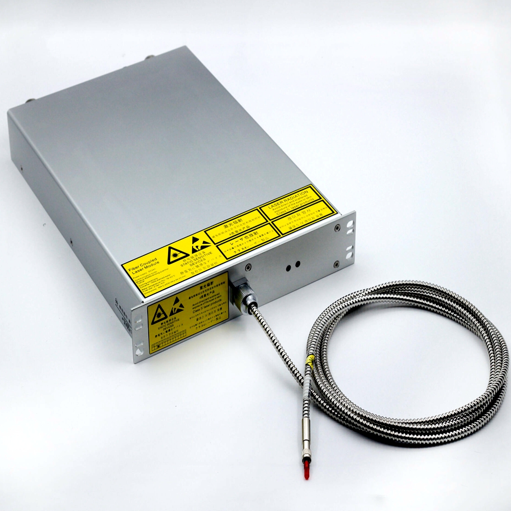
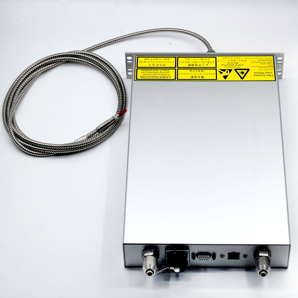
375nm 10W Fiber Coupled Laser for LDI Exposure Machine
Wavelength: 375nm
Output Power: 10W (CW)
Working Voltage: 24V
Fiber Core Diameter: 105um , NA0.22, 1.5M length
Coupling Efficiency: 85%
Housing Size: 35423044mm (Customizable)
Life Time:10,000 hours
Powerful UV Laser 375nm 10W Fiber-Coupled is industrial grade solution for high-throughput UV processing.
Combining 375nm UV-A wavelength material absorption, 10W ultra-stable output.
Keys for Industrial UV Processing
1.375nm UV-A Wavelength: Universal Material Compatibility
375nm wavelength (±5nm tolerance) aligns with absorption peaks of epoxy/acrylic-based photoresists, solder masks, UV inks, and polymers—ensuring rapid photopolymerization without material degradation.
Outperforms longer UV wavelengths (385nm/395nm) in curing efficiencyand shorter UV-C (≤280nm) in penetration depth (up to 100μm), ideal for thick-film curing and deep-layer material processing.
Superior absorption on non-ferrous metals (copper, aluminum) and semiconductors for UV-induced surface modification and micro-structuring.
2. 10W High Power + Water Cooling: 24/7 Stable Operation
10W CW output with lower power fluctuation over 24 hours, delivering energy density ≥10,000mW/cm² at the fiber tip—reducing processing time by 80% compared to 2W modules.
Efficient water cooling system with adjustable flow rateand temperature control (20°C~30°C), ensuring junction temperature ≤75°C during continuous operation.
Eliminates thermal drift and power decay common with air-cooled high-power modules, supporting uninterrupted industrial production lines.
Key Industrial Applications:
PCB Manufacturing: High-speed solder mask curing (rigid PCBs, FPCs, HDI boards), photoresist exposure for fine-patterning.
UV Curing: Conformal coating curing, UV inkjet printing, adhesive bonding in electronics/automotive assembly.
Microfabrication: Precision structuring of polymers, glass, and thin films for MEMS, microfluidics, and semiconductor components.
Material Processing: UV-induced surface modification (hydrophilic/hydrophobic treatment), polymer aging testing, and nanomaterial synthesis.
3D Printing: High-power light source for large-format SLA/DLP 3D printers, enabling fast curing of thick resin layers.
An LDI (Laser Direct Imaging) exposure machine is a high-precision, non-contact system used in PCB and screen printing to directly project circuit or image patterns onto photoresist-coated substrates, eliminating the need for traditional photomasks. It uses UV lasers, usually at 405nm, and DMD (Digital Micromirror Device) technology to achieve high-resolution imaging, improving accuracy, reducing labor, and facilitating rapid prototyping for HDI boards.
video shows how a laser direct imaging machine creates circuit patterns on a PCB.