GaInP/GaInAsP red semiconductor laser epitaxial wafer
Epitaxial wafers of custom sizes and thicknesses are available.
Some parameters can be customized according to customer requirements.
3/4inch diameter
Thickness 450+-25um
PL wavelength 780-860nm
surface orientation
(100) 15°Off Toward
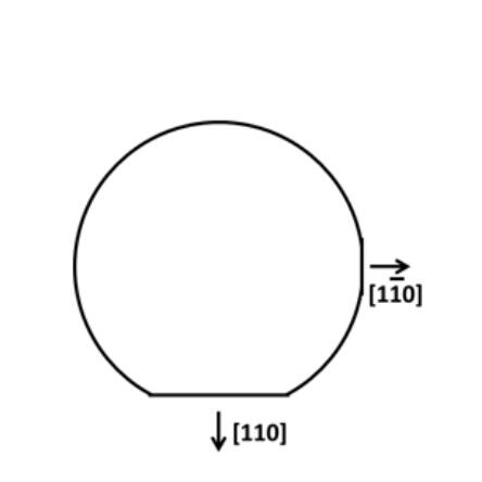
Positioning Edge Standard US
Substrate EPD <500 cm-2
Name Material Thickness Doping Concentration (cm-3)
Ohmic contact layer GaAs 2000~3000 >1E+19
Band gap transition layer GaInP 200~500 1~5E+18
P confinement layer AlGaInP 9000~11000 1~2E+18
Waveguide layer GaInP 3000~6000 -
Active region InGaAsP ~100 -
Waveguide layer GaInP 3000~6000 -
N confinement layer AlGaInP 9000~11000 0.5~1E+18
Transition layer GaAs ~3000 1~4E+18